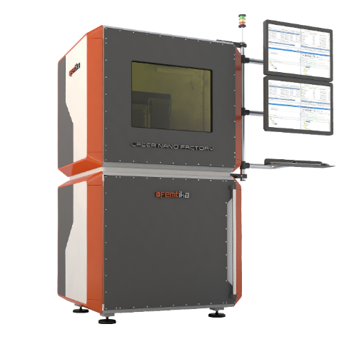
Laser Nanofactory - Femtosecond laser hybrid micro-fabrication workstation
Our Laser Nanofactory combines additive and subtractive manufacturing
Laser Nanofactory allows 3D fabrication of almost any imaginable shape micro-strucutres and the ability to cut and drill in micro-scale without damaging the surrounding material.

Features
What makes this product special?
2 Provide stitching error free manufacturing without sacrificing the speed or the quality
2 Combines two different 3D fabrication technologiesadditive and subtractive manufacturing
2 Uses femtosecond laser with tunable parameters
-  Simultaneous motion of galvo and servo axes over the entire working field (110 x 110 x 60 mm).
- Uses femtosecond laser, with tunable parametres.
- Allows customer to modify system according to specific needs and requirements.
- Ultra short laser pulses allow extremely high intensities – very clean ablation edges can be reached.
- Provides stitching error free manufacturing without sacrificing the speed or the quality.
- Combines two different 3D fabrication technologies: additive and subtractive manufacturing.
- Enables the fabrication of micro-nano structures using wide range of materials.
- Typical working speed - 15 mm/s (up to 50 mm/s).
- Integrates nano-structures into existing micro- or macro- structures (in- situ).
- Perfect for producing arbitrary high- resolution 3D microstructures.
Continuous wave / Nanosecond / Femtosecond
Ultrashort pulses, compared to nanosecond and continuous wave lasers, deliver energy very quickly, resulting in high peak intensities.
Specifications
Additive manufacturing
Based on multiphon-photopolymerization process. Various polymers can be used.
Subtractive manufacturing
Includes laser ablation and selective laser etching technologies. Suitable materials: glass, metals, polymers.
Other technologies
Laser welding in micro-scale, scribing, microstructures in-situ.
Laser
Amplified femtosecond laser in user selected configuration. Wavelengths: 1030 nm and 515 nm. Max. average power: 4W@1030 nm and 2.7W@515 nm. Pulse duration: 290 fs - 10 ps.
Nanopositioning
Linear stages with synchronized galvanoscanners.
Beam delivery and control
Power control: acousto-optical modulator + motorized attenuator; power monitoring: integrated powermeter; focusing optics: set of microscope objectives - NA up to 1.4.
Cases
Discover how our technology helped overcome some of the industries challenges
??????Case 1
??CHALLENGE:??
Producing of photonic devices based on high-resolution (up to hundreds of nm) single features for applications in visible and IR part of the spectrum.????
??SOLUTION:??
??By applying ultra-sharp focusing (NA up to 1.4), low shrinkage SZGel and advanced fabrication techniques repeatable production of structures with sub 200 nm features and sub 400 nm periodicity are possible.??
?

??Case 2??
CHALLENGE:
Creation non-deformed complex 3D structures with intricate internal geometry and strong attachment to the substrate.
SOLUTION:
Using the material with limited post-development shrinkage (like SZGel) allows preserving fabricated shape through all manufacturing procedures. Furthermore, this material has excellent adhesion.

Case 3
CHALLENGE:
Manufacturing of relatively large (from tens of μm to cm) structures with fine (hundreds of nm) internal features.
SOLUTION:
Tuning of Numerical Aperture (NA) during fabrication opens a simple way for on-the-fly resolution control. Therefore, parts that are bulky and do not require high resolution (>1 μm feature size) can be created using lower NA (<0.8), while fine features (sub 1 μm) with high NA (0.8<).

Case 4
CHALLENGE:
Free movable structure fabricated without addtional supports or stitching.
SOLUTION:
SZGel is hard gel form during fabrication, which allows it to act as a support for already produced parts of the object during fabrication. Coupled with linear stage-galvano-scanner combination it allows to create structures without additional supports or stitching.

Case 5
CHALLENGE:
Fabrication of precise structures (nm-μm fidelity) that are relatively big in overall size (mm-cm). Such components should be mechanically rigid and transparent in the spectrum range from UV to IR.
SOLUTION:
Selective laser etching in fused silica (mechanically rigid and clear in wide spectral range (from UV to near IR)). What is more, as fused silica does not exhibit development-induced shrinkage there are minimal deviations from the initial model and almost no limitations in overall size.

Case 6
CHALLENGE:
Fabrication of mechanically flexible structures in microscale.
SOLUTION:
Functional intertwined geometries such as “chain-mail” allow creating structures out of hard material (for instance SZGel) that are flexible in-macro scale. SZGel simplifies this task because it provides a possibility to create such intricate structures without additional supports.

Case 7
CHALLENGE:
microscaffolds with high aspect ratio features and arbitrary 3D geometry out of biocompatible material.
SOLUTION:
The amplified fs laser system employed in the fabrication setup allow photoinitiator-free structuring of SZGel, which results in greatly increased biocompatibility of a material and high resolution of produced features.

Case 8
CHALLENGE:
Fabrication of microoptics of any desirable shape as the optimized surface geometries allow minimising aberrations or creating exotic light distributions, like, for instance, Bessel beams or optical vortexes.
SOLUTION:
Coupling the superb positioning accuracy with high resolution fabrication enables arbitrary shaped profiles of microlenses surface roughness suitable for optical applications.

Case 9
CHALLENGE:
Production of large arrays of mechanically robust microneedles, that could be used for micro-hole puncturing.
SOLUTION:
Our technology allows fabrication of microstructure arrays in excess of cm (working field - 110 x 110 x 60 mm). The needles can be produced using different technologies (3D laser lithography, selective glass etching, ablation) which enables to choose material (glasses, polymers, ceramics, metals).

Case 10
CHALLENGE:
Microfluidic systems containing elements with different shapes and sizes.
SOLUTION:
When using selective laser etching it is possible to inscribe all the components of the system during one technological step. Technology allows to produce microfluidical systems out of fused silica which has broad transparency window, is optically and chemically inert, mechanically robust.

Case 11
CHALLENGE:
3D objects in range of hundreds of μm combining arbitrary shape, high aspect ratio, fine and/or suspended structures.
SOLUTION:
High precision positioning combining liner stages and galvano-scanners allows stitchless structuring of objects in range of hundreds of μm. Combined with high mechanical strength and hard gel form of SZGel it allows to incorporate suspended, fine and high-aspect ratio features into relatively large objects.

Case 12
CHALLENGE:
3D structure of arbitrary geometry on the fiber tip.
SOLUTION:
Special holder allows fixing fiber in the fabrication system. This way any kind of 3D structure can be fabricated on the fiber tip.

Case 13
CHALLENGE:
Clear laser ablation edges in ceramics.
SOLUTION:
The laser ablation made in ceramics with fs laser (on the left) and with ns laser (on the right): when using ns laser, the ablation edges are melted and some cracks have appeared. Opposite to this, the ablation edges made with fs laser are clean, without any damage of material.