Nuohai Optical attends 20th China International Optoelectronic Exposition, at Shenzhen (CIOE 2018)
-a2c5764a-a3a2-444f-9283-7cf41f77e508.jpg)
SHENZHEN, China, Sep. 5th 2018 – Sep. 8th2018, 20th China International Optoelectronic Exposition was successfully launched. Nuohai Optical presented the core products during the exhibition. LightFab GMBH - 3D Printer、Omega/Theta XRD from Freiberg Instrument GMBH、The Desktop X-ray Diffractometer for Crystal Orientation Measurement (DDCOM)、Laser labelling with the SIM marking system from GMBH、Bruker - Stylus Profilers、Bruker - Contour GT-K 3D Optical Microscope. As well as the custom processing service from LightFab 3D Printer.
Nohai Optical Instrument Equipment (China) Co., Ltd. aimed to provide optical researchers and enterprises with the instruments and manufacturing services of glass micro-parts. Including production of prototype, small batch and large batch. Nuohai also provide micro-machining of complex glass parts, such as the mass production of precision parts for medical diagnosis and the production of optical molds, etc.
The LightFab 3D Printer is specially designed for our subtractive 3D printing process SLE (selective laser-induced etching) and is also used for other 3D laser writing processes inside transparent materials like wave guide writing, 2-photon-polymerization, backside ablationand crack-free markings. We integrate our system technology into your production line and offer special machines enabling even mass-production of 3D parts. In addition, we support you in process development for special structures, new materials as well as higher throughput.
-8cd9a3e2-7e44-4648-adc1-660891548cbe.jpg)

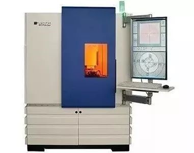
LightFab - 3D Printer
Our LightFab 3D laser Printer consists of a high dynamic 3D Microscanner, a high precision 3-axis system for stepping, fs-laser, camera andvision system for automatic alignment, laser safety and an innovative CAD/CAM/nc software package in one housing: LightFab 3D Printer. The LightFab 3D Printer is specially designed for oursubtractive 3D printing process SLE (selective laser-induced etching) and is also used for other 3D laser writing processes inside transparent materials like waveguide writing, 2-photon-polymerization, backside ablation andcrack-free markings. We integrate our system technology into your production line and offer special machines enabling even mass-production of 3D parts. Inaddition we support you in process development for special structures, new materials as well as higher throughput.
Fraunhofer Institute for Laser Technology ILT and Fraunhofer Institute for Silicate Research ISC together with Lightfab from Aachen are developingan entirely new process chain for the manufacturing of three-dimensional devices. It is perfect for Direct Laser Writing processes such as multi photonpolymerization of 3D polymer micro structures, 3D waveguide writing by ultra fast laser inscription, 3D lithography in glasses and crystals by selective laser-induced etching, internal welding of glass, and micro structuring by precision ablation with e.g. 1 um focus diameter.
The LightFab 3D laser Printer is designed for fastest automatic 3D printing with the included CAD/CAM software. Advantages of SLE are the large precision (~1um), no debris, true 3D capability and the high processing speed using our LightFab 3D Printer. In cooperation with Fraunhofer ISC, the two-photon polymerization technology is combined with SLE technology to realize the processing of complex structures such as curved surfaces and curved channels.
Applications
LightFab3D laser printer can be used for applications such as micro fluidics, micro mechanics, integrated optics and other applications that require high precision, high resolution 3D microstructures. E.g. cell sorter, microfluidical cross-section chip, rotatable gear, M1 threaded hole in quartz glass, microchannel, 3D nozzles in quarts glass and so on.

Introduction
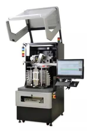
of Omega/Theta XRD from Freiberg Instrument GMBH
The
Omega/Theta X-ray diffractometer is a fully automated vertical three axes
diffractometer for orientation determination for various crystals using
Omega-Scan and Theta-Scan methods and rocking curve measurements. All
measurements are automated and can be accessed from the user-friendly software
interface. Using the Omega Scan, the complete lattice orientation can be
determined in on crystal rotation.
Omega/Theta XRD
For ultra-fast crystal orientation and rocking curve measurements
Ultra-fast crystal orientation measurement using Omega-scanmethod (up to 5s)
Fully automated complete lattice orientation measurement ofsingle crystals
Automated rocking-curve measurement
High precision up to 0.001°
Additional sample rotation axis for 3D mapping
Laser scanner for sample shape measurement

-b6c33582-b872-4b9e-912d-dbd6e043692f.jpg)
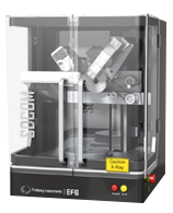
DDCOM
The DesktopX-ray Diffractometer for Crystal Orientation Measurement (DDCOM) is an automated tool to determine the orientation of various crystals using the ????Omega-scan method????.
High precision:up to 0.01°
Suitable for a unique variety of materials in a large rangeof size and weight, such as: Wafers from 2-12” and Ingots up to 20kg
Easily movable and light weight desktop design
Determination of entire crystal orientation within 5seconds
Low energy consumption and operating costs due to aircooled X-ray tube (no water cooling required)


SDCOM
SmartX-ray Diffractometer for Crystal Orientation Measurement (SDCOM), especially designed for small crystals
Able to measure very small crystals down to 1 mm orlarger samples
Variety of sample holders and transfer fixtures towardswire saw, grinding, etc.
Marking option of lateral crystal direction
Air cooled X-ray tube, no water cooling required
Highest precision: 0.01°


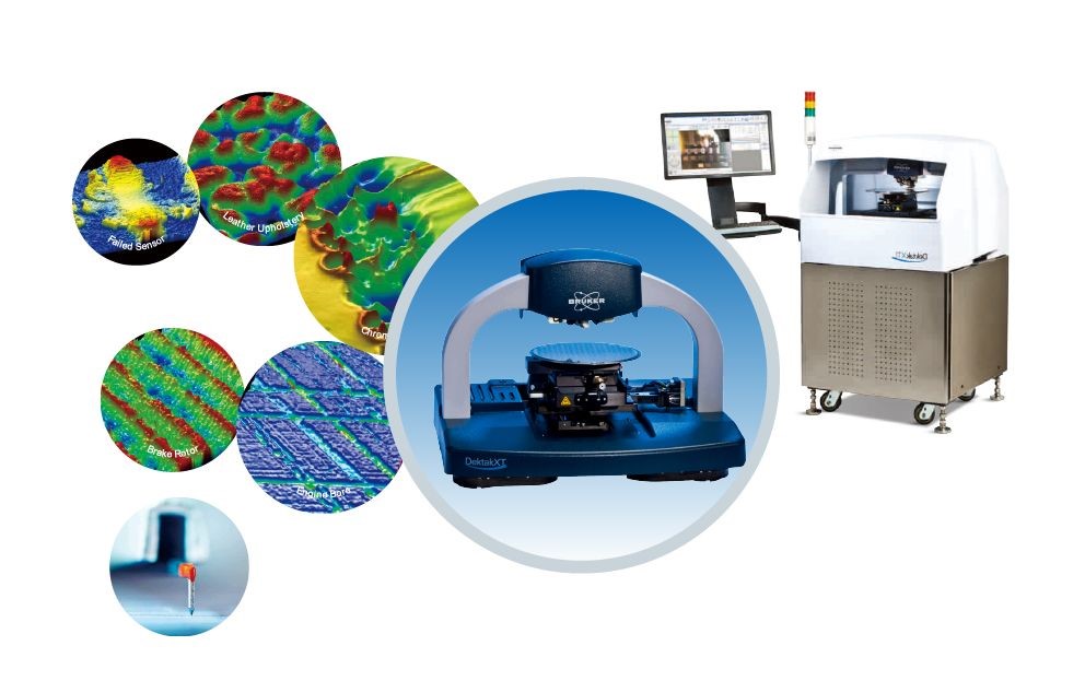
Bruker - Stylus Profilers
Bruker's DektakXT Stylus Profiler features a revolutionary design that enables 4a ngstrom repeatability. This major milestone in stylus profiler performance isthe culmination of forty years of Dektak innovation and industry leadership.Through its combination of industry firsts, DektakXT delivers the ultimate in performance, ease of use and value to enable better process monitoring from R&D to QC. The technological breakthroughs incorporated in Dektak enable critical nanometer-level surface measurements for the microelectronics, semiconductor, solar, high-brightness LED, medical, and materials science industries.


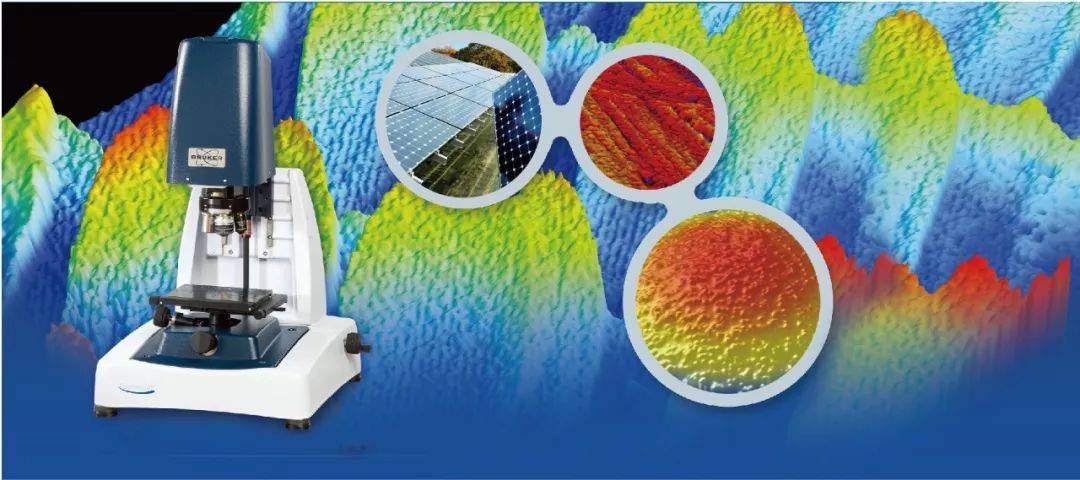
Bruker - ContourGT-K 3D Optical Microscope
The
ContourGT-K 3D Optical Microscope is the standard in capability and value for
surface profilers. With a variety of 2D/3D measurements, high-resolution
imaging, and a user-friendly interface, the system offers uncompromised
metrology in a simplified package with a compact footprint.
ContourGT-K
is the ideal measurement system for labs with basic metrology and imaging
needs.


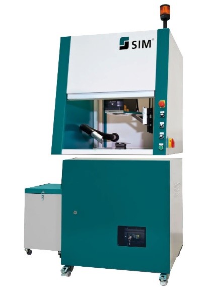
Laser labelling with the SIM marking system from GMBH
Ourlaser labelling system provides self-contained and high-performance solutionsfor laser labelling small batches of individual parts. The"STANDARD", “BASIC” and “ADVANCED” laser marking system versions canbe set up directly on a desk or mounted onto the moveable base frame. By usingthe most up-to-date 3-axis laser marking systems, we are able to offer you a laser labelling system that can be precisely adjusted to the materials and partgeometry you wish to label.
The integrated optical “3-axis technology” in the SIM laser marking systems, which allows the focal point to be freely set, is especially impressive. This allows the marking laser to follow various shapes, easily switch between different heights (± 21 mm = 42 mm) and sharply mark any shape, including slanted surfaces, cylinders and cones.
Depending on the type of laser, the size of the labelling field varies between 120 x 120 mm to 330 x 330 mm.
Various laser marking systems for different types ofmaterials, including systems with power ratings of between 13 and 50 W:
CO2 laser with a wavelength of 10,600 nm
YVO4 laser with a wavelength of 1,064 nm
Fibre laser with a wavelength of 1,090 nm
Application:Mental, plastic, ceramic、Paper、PCB、Wafer


-a2c5764a-a3a2-444f-9283-7cf41f77e508.jpg)
-8cd9a3e2-7e44-4648-adc1-660891548cbe.jpg)


-b6c33582-b872-4b9e-912d-dbd6e043692f.jpg)
